

SOLUTION
SCROLL DOWN

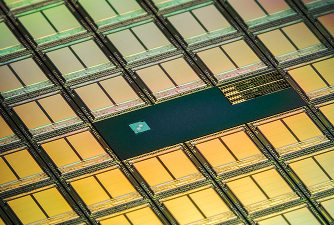



Flip Chip Bonding Solutions
Co-Packaged Optics (CPO) High-Speed Optoelectronic Co-Packaging Integration Solutions
Flip Chip Bonding technology directly connects a chip to a substrate or package structure with the active surface facing downward. This approach significantly shortens signal transmission paths while enabling high I/O density, miniaturization, and high-performance integration, making it widely applicable to high-performance computing, advanced packaging, and high-density electronic component integration.
As chip performance continues to increase, advanced packaging structures require greater signal integrity, thermal performance, and interconnect density. High-density flip chip bonding requires not only precise control of the relative positioning between the chip and substrate, but also careful management of bonding pressure, temperature, and process consistency to ensure packaging quality and long-term reliability.
NexBond Systems leverages its expertise in high-precision bonding equipment to provide stable and highly integrated solutions for precision alignment and bonding processes in flip chip packaging. Through precision mechanical design, intelligent control, and process parameter management, our solutions help customers improve bonding accuracy and process stability while meeting the manufacturing requirements of high-density and high-performance packaging.
With the rapid development of AI, HPC, HBM, and advanced semiconductor applications, packaging technology has become a critical factor in overall system performance. NexBond Systems continues to advance high-precision bonding technologies across R&D, equipment manufacturing, and process applications, helping customers establish more efficient and reliable flip chip packaging processes.
- Solution Details
Flip Chip Bonding technology directly connects a chip to a substrate or package structure with the active surface facing downward. This approach significantly shortens signal transmission paths while enabling high I/O density, miniaturization, and high-performance integration, making it widely applicable to high-performance computing, advanced packaging, and high-density electronic component integration.
As chip performance continues to increase, advanced packaging structures require greater signal integrity, thermal performance, and interconnect density. High-density flip chip bonding requires not only precise control of the relative positioning between the chip and substrate, but also careful management of bonding pressure, temperature, and process consistency to ensure packaging quality and long-term reliability.
NexBond Systems leverages its expertise in high-precision bonding equipment to provide stable and highly integrated solutions for precision alignment and bonding processes in flip chip packaging. Through precision mechanical design, intelligent control, and process parameter management, our solutions help customers improve bonding accuracy and process stability while meeting the manufacturing requirements of high-density and high-performance packaging.
With the rapid development of AI, HPC, HBM, and advanced semiconductor applications, packaging technology has become a critical factor in overall system performance. NexBond Systems continues to advance high-precision bonding technologies across R&D, equipment manufacturing, and process applications, helping customers establish more efficient and reliable flip chip packaging processes.